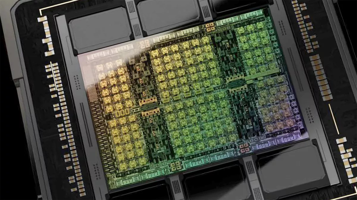
Nvidia may be joining AMD and Intel in developing a multi-chiplet architecture for its next generation of GPUs, and could reap major gains in terms of performance.
Nvidia is the last of the big three chipmakers that still uses a single slice of silicon for the processors inside its best graphics cards, so it’s something of a welcome surprise that rumors have begun circulating that the company will finally move to the more adaptable multi-chiplet module (MCM) design with its next-generation Nvidia Blackwell architecture.
The report comes from well-known hardware leaker @kopite7kimi on X, who said that Nvidia’s commercial-grade GB100 GPU will feature MCM for the first time.
After the dramas of GA100 and GH100, it seems that GB100 is finally going to use MCM.September 18, 2023
The Nvidia Blackwell architecture is expected to power both Nvidia’s next-gen commercial GPU products, which are used by data centers and industial-scale users, as well as its consumer graphics cards, the Nvidia RTX 5000 series.
Even though both will use the Blackwell architecture, however, it’s unclear at the moment if the MCM shift will also extend to the Nvidia 5000 series graphics cards. If it does, though, it could provide the transformational performance for Nvidia’s next graphics card generation that was often lacking in some of its more recent RTX 4000-series cards.
The chiplets in an MCM design, when interconnected into a single processor, promises significantly faster performance over a monolithic slab of silicon. As Tom’s Hardware explains, a single silicon chip is constrained by the physical dimensions of the equipment used to fabricate it. Currently, the process Nvidia uses can only produce a 26mm by 33mm (858mm²) pieces of silicon at most, and Nvidia’s commercial-grade GPUs are already bumping right up against that maximum size.
And since it’s become exponentially more difficult to further shrink the size of a transistor, the electronic switch inside a chip that produces a computer’s logic functionality, the only way to increase the number of transistors in your GPU to increase performance is to make the chip larger than the physical manufacturing process will allow.
That’s where the chiplets come in. If you can produce two or more chiplets that are smaller, but use special ties called interconnects to link them together so they act as a single unit, you can effectively build a larger chip than the fabrication process can supprt and dramatically improve performance. With an MCM design for its GPUs, Nvidia might be able to deliver the kinds of gains across its entire portfolio of Nvidia 5000 series cards that many were hoping to see with the 4000 series but which Nvidia wasn’t able to deliver consistently.
Obviously, this is still very speculative and based on rumors, but there’s a reason why both AMD and Intel have made the switch to MCM in their GPUs and CPUs, and Nvidia would be very smart to follow suit, or risk getting left behind.
Make the move to MCM, Nvidia, it’s the only way forward

The problem chip makers have been having for years now has been the end of Moore’s Law, the famous prediction by Intel co-founder Gordon Moore that transistor density on a chip would double roughly every two years.
For 50 years, that had been the case, but as we now measure the size of transistors relative to the diameter of individual atoms in the silicon, cutting a transistor’s size in half just isn’t possible anymore.
But consumers and industry have become used to faster computers every couple of years, and so no one really wants to hear that the party is over. If you’re a chip maker looking to keep selling more processors, you have to find another way to deliver those performance gains the market expects, Moore’s Law be damned.
The answer to this is using multiple chips in conjunction with one another to achieve those performance targets. We’ve already been doing this for more than a decade, as Nvidia well knows.
There was a time when there was no such thing as a graphics processor, there was just the main CPU which was expected to handle graphics as well as every other operation.
As graphics became more advanced though, this so heavily taxed the CPU that something had to be done before computing 3D scenes either ate up 99.9% of the CPU’s clock cycles, or the limits of the CPU itself ground computer graphics progress to a halt.
The work around was to pass all but the most basic graphics processing work off to a second processor, the GPU, which was specially designed for this task and which went on to power the modern era of computer graphics. Nvidia knows this because it was the one that created the world’s first GPU, the Nvidia GeForce 256, back in 1999.
We’ve come full circle then, and graphics processors are so overwhelmed with the workloads being assigned to them that they cannot keep up and we can’t squeeze more performance out of the same-sized silicon. It’s time then to break up geometry, rasterization, ray tracing, machine learning, and other GPU workloads into different mini-processors that can be specifically engineered to perform those tasks faster and more efficiently than we’re currently doing.
Nvidia’s chief competitor, AMD, is already doing this and it’s seen very positive results so far. And while the first few attempts to get MCM engineering right might not be the revolution that the first GPU was when it landed over 20 years ago, future attempts will get us to where we want—and Nvidia needs—to be, so Nvidia should probably get to work on that.


