

Apple’s branding for the A18 and A18 Pro chips.
New microphotography of the A18 and A18 Pro chips reveal the inner workings of the iPhone 16 line’s chips, as well as confirming Apple isn’t using chip binning right now.
Apple’s chips in its products are impressive, giving other processor makers a run for their money over the years. As the designs improved, so did the performance and capabilities of its hardware, as is evident in the iPhone 16.
Following after teardowns, the next logical step is to closely examine the chips, and Chipwise has done just that. It has published photographs of the dies used in the A18 and A18 Pro.
The packaging of the chip has been consistent over the years, with TSMC using an Integrated Fan-Out Package-on-Package (InFO-PoP) method for a while. The technique stacks a DRAM package on top of the SoC die, with high-density redistribution layers and a Through InFO Via assisting to create a compact overall chip size.
In other words, Apple stacks the memory on top of the CPU and GPU, instead of having them in a separate die.
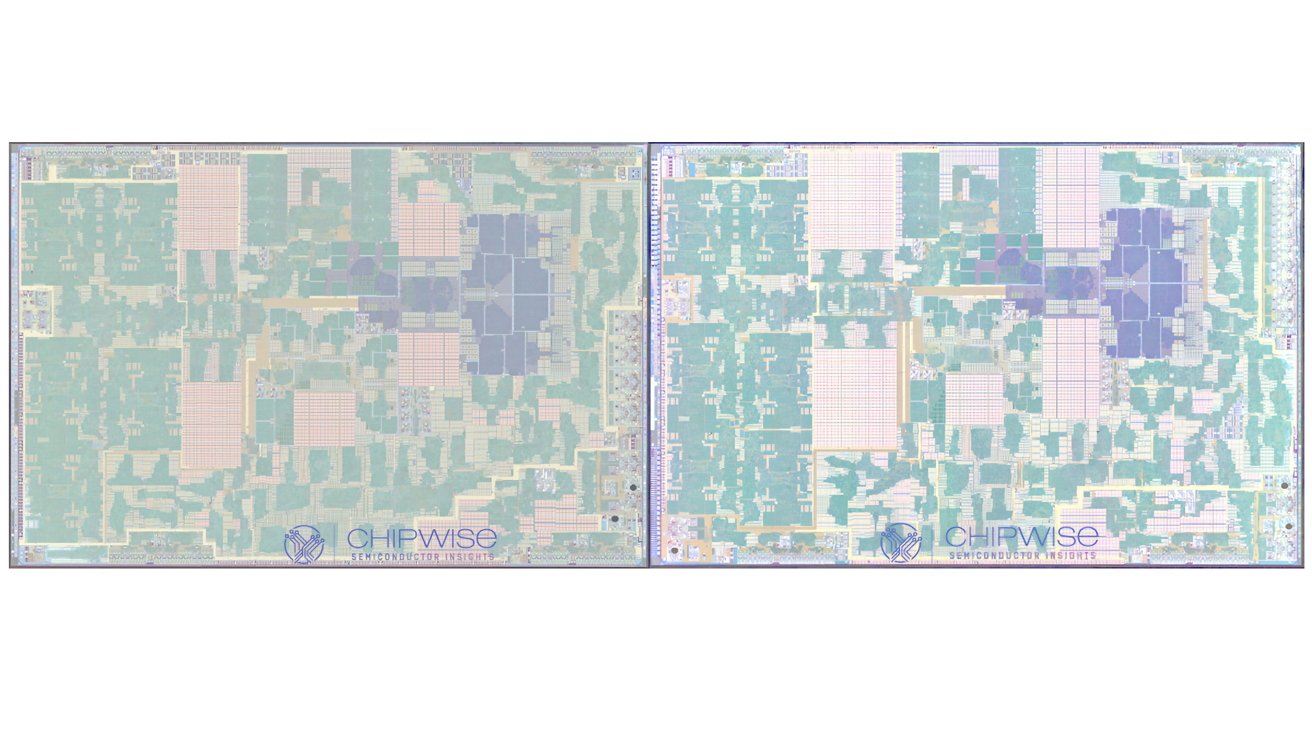
Die shots of the A18 (left) and the A18 Pro (right0 [via Chipwise]
The shots of the A18 SoC shows off its 3-nanometer manufacturing process, and a fairly straightforward layout. Cores and other elements are clustered together, almost like fields in an overhead shot of a countryside landscape.
Checking over the die shot for the A18 Pro, it does at first glance appear to be very similar to the A18’s version. You can see where clusters are placed in similar locations, and it would be quite easy to mistake one for the other from these images alone.
However, a more careful examination shows that Apple has included a lot more transistors on the A18 Pro. Many of the lighter sections take up a lot more space on the die compared to what’s on the A18.
The images at least prove that Apple isn’t simply performing chip binning. This is a process where a Pro chip would be made, but faulty versions with a failed core could be repackaged as non-Pro A18 chips instead.
It was believed that the A18 was going to be a binned version of the A18 Pro, since it relies on one fewer GPU core. With similar features like Apple Intelligence support and hardware-based ray tracing, it was easy to believe chip binning was at play.
With the differences evident in the shots, it seems that Apple is legitimately designing and producing two different chips, instead of relying on chip binning.


